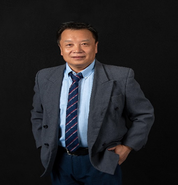
Li Shunpu, Distinguished Professor
Profile:
Li Shunpu, doctor, is a Distinguished Professor. He received his bachelor's and master's degrees in physics from Lanzhou University in 1987 and 1990, respectively. After receiving his doctorate in 1993 (in collaboration with the Institute of Metal Physics of the former Soviet Academy of Sciences), he stayed at the Institute of Physics of the Chinese Academy of Sciences as a research assistant. From 1998-2002 he was a postdoctoral researcher at Cavendish Laboratory and Nano Centre, Cambridge University. He started his industrial research career in 2003, working as a Senior Researcher and Senior Engineer at EPSON Cambridge Laboratories, Cambridge Display Technologies and the National Institute of Tyndall. In 2013, he was a Maria Curie Senior Research Fellow at the Faculty of Engineering, University of Cambridge, funded by a European Community Research Grant. His research interests include semiconductor physics and devices, micro- and nanomaterials processing, and spintronic materials. He has obtained 28 patents on inventions, co-authored four monographs, and published more than 60 papers as first author or corresponding author in various prestigious journals (Nature, Advanced Materials, Physical Review Letters, etc.). He is currently working on the general program of the National Natural Science Foundation, the general program of the Guangdong Provincial Natural Science Foundation and the innovation team program of the Guangdong Provincial Department of Education. He has been in charge of two European national projects and one European community project.
Academic Background:
September 1990 - June 1993, Chinese Academy of Sciences, Institute of Physics, Doctoral Candidate
September 1987 - June 1990, Lanzhou University, Faculty of Physics, Master
September 1983 - June 1987, Lanzhou University, Faculty of Physics, Bachelor
Work Experience:
November 2018 - Present Shenzhen Technology University, School of New Materials and New Energy, Distinguished Professor
January 2013 - November 2018 University of Cambridge, Faculty of Engineering, Maria Curie Senior Research Fellow
February 2009 - November 2012 Tyndall National Research Institute, Senior Research Fellow
January 2008 - January 2009 Cambridge Display Technologies, Senior Engineer
March 2003 - December 2007 Epson Cambridge Laboratory, Senior Research Fellow
July 1998 - February 2003 University of Cambridge, Cavendish Laboratory, Nano Centre, Postdoctoral Fellow
September 1993 - July 1998 CAS Institute of Physics, Research Associate
Research Interests:
1. Magnetic thin films and magnetic memory devices
2. Organic semiconductor components (OTFTs, OLEDs, OPVs)
3. Micro- and nano-processing technologies (photolithography, nanoimprinting, soft lithography, self-assembly)
Research Projects:
1. Polymer Organic Semiconductor Field Effect Tube and its Application in Flexible Display, Guangdong Provincial Natural Science Foundation, General Program, 2019A1515011673, 2019 - 2022.
2. Self-aligned high-resolution organic ferroelectric transistor based complementary memory, EU FP7, 301028, 2013-2015.
3. Textured dye sensitized solar cell, Enterprise Ireland, CF/2011/1616, 2011- 2013.
4. A novel process for printed electronics: all self-aligned, printed thin film transistors defined by embossed triple banks,Enterprise Ireland, PC/2009/0215, 2009-2011.
Representative Papers:
1. E. Tan, P. Shrestha, A. Pansare, S. Chakrabarti, S. Li, D. Chu, C. Lowe, A. Nagarkar. Density modulation of embedded nano-particles via spatial Adv. Mater. 51, 1901802 (2019)
2. S. Li et al. Two-dimensional arrays self-assembled via interference of concentration modulation waves in drying solutions Materials Horizons 6,507 (2019).
3. S. Li et al. High-resolution patterning of solution-processable materials via externally engineered pinning of capillary bridges Nat. Commun. 9, 393(2018).
4. J. Wu, Y. T. Chun, S. Li et al. Broadband MoS2 field-effect phototransistors: ultrasensitive visible-light photoresponse and negative infrared photoresponse Adv. Mater. 30,1705880(2018).
5. W. Liu, L. He, Y. Xu, K. Murata, M. Onbasli, M. Lang, N. Maltby, S. Li, X. Wang et al. Enhancing magnetic ordering in Cr-doped Bi2Se3using high-TC ferrimagnetic insulator Nano Lett. 15, 764 (2015).
6. S. Li, W. Chen, D. Chu, S. Roy. Self-aligned, high resolution printed polymer transistors Adv. Mater. 23, 4107 (2011).
7. W. S. Lew, S. Li, L. Lopez-diaz et al. Mirror domain structure induced by interlayer magnetic wall coupling Phys. Rev. Lett. 90, 217201(2003).
8. S. Li, W. S. Lew, J. A. C. Bland et al. Magnetic domain confinement by anisotropy modulation Phys. Rev. Lett. 88, 87202 (2002).
9. S. Li, W. S. Lew, J. A. C. Bland et al. Spin-engineering magnetic media Nature 415, 600(2002).
10. S. Li, D. Peyrade, M. Natali et al. Flux closure structures in cobalt rings Phys. Rev. Lett. 86, 1102(2001).
Representative Patents:
1. S. Li, C. Newsome, T. Kugler and D. Russel, Method of fabricating a desired pattern of electronically functional material, US2005250244.
2. S. Li, T. Kugler, C. Newsome and D. Russel, A self-aligning patterning method for use in the manufacture of a plurality of thin film transistors,US2006128076.
3. S. Li, C. Newsome, D. Russel and T. Kugler, A patterning method for fabricating high-resolution structures, US2006194444.
4. S. Li, C. Newsome, D. Russel and T. Kugler, Organic electronic device fabrication by micro-embossing, US2006/0280021.
5. S. Li, C. Newsome, D. Russel and T. Kugler, Thin film transistor and method for fabricating an electronic device,US2007/0082438.
6. S. Li, C. Newsome, D. Russel,T. Kugler,and D. Russell,Patterning of electronic devices by brush painting onto surface energy modified substrates, US2007/0105396
7. S. Li and I. Masaya, Electrochemical cell and method of manufacture, US2007119048.
8. S. Li, C. Newsome, D. Russel and T. Kugler, Device fabrication by ink-jet printing materials into bank structures with multi-leveled thickness contrast, US2007287270.
9. S. Li, C. Newsome and D. Chu, Novel methods of bank structure fabrication for ink-jet printing,US2008006161.
10. S. Li, C. Newsome and D. Chu, Method for forming surface energy difference bank, patterning method, bank structure, electronic circuit, electronic device, and electronic apparatus, US2008017606 (A1).
Contact Information:
E-mail:lishunpu@sztu.edu.cn