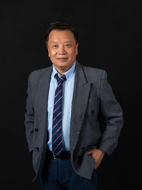
李顺朴 特聘教授
个人介绍:
李顺朴,特聘教授、分别在1987年和1990年于兰州大学物理系获学士和硕士学位,1993年于中科院物理所获得博士学位,后留所工作任助理研究员。1998年至2002年在剑桥大学卡文迪许实验室和纳米中心做博士后研究。 于2003年开始从事工业研究,先后在EPSON(爱普生)剑桥实验室,剑桥显示技术公司,丁达尔国家研究院任高级研究员和高级工程师。于2013获欧共体科研基金资助在剑桥大学工程系任玛丽亚-居里高级研究员。研究工作涉及多个领域,包括半导体物理与器件,微/纳米材料加工, 自旋电子材料等。 获发明专利28项,参与了四部专著的撰写,在各种权威刊物上(Nature, Advanced Materials, Physical Review Letters etc.)发表论文70多篇。目前在研的主要项目有国家自然基金面上项目,广东省自然基金面上项目,广东省教育厅创新团队项目。
教育背景:
1990.09-1993.06 中科院物理所,博士研究生
1987.09-1990.06 兰州大学,物理系,硕士
1983.09-1987.06 兰州大学,物理系,本科
工作经历:
2018.11-至今 深圳技术大学,新材料与新能源学院,特聘教授
2013.01-2018.11 剑桥大学,工程系,玛丽亚-居里高级研究员
2009.02-2012.11 丁达尔国家研究院,高级研究员
2008.01-2009.01 剑桥显示技术公司,高级工程师
2003.03-2007.12 爱普生剑桥实验室,高级研究员
1998.07-2003.02 剑桥大学卡文迪许实验室/纳米中心,博士后
1993.09-1998.07 中科院物理所,助理研究员
研究方向:
1. 有机半导体材料与器件
2. 微纳加工
科研项目:
1. 有机半导体薄膜溶液内斑图的生成与生长动力学研究,国家自然科学基金面上项目, 12274303, 2023-2026.
2. 功能薄膜与电子器件,广东省教育厅创新团队项目,2021KCXTD045, 2021-2024.
3. 聚合物有机半导体场效应管及其在柔性显示中的应用,广东省自然科学基金面上项目,2019A1515011673,2019-2023.
代表论文:
1. C. Zhao, R. Ma, Y. Hou, L. Zhu, X. Zou, W. Xiong, H. Hu, L. Wang, H. Yu, Y. Wang, G. Zhang, J. Yi, L. Chen, D. Wu, T. Yang, G. Li, M. Qiu, H. Yan, S. Li, G. Zhang. 18.1% ternary all-Polymer solar cells sequentially processed from hydrocarbon solvent with enhanced stability. Adv. Energy Mater. 13, 2300904 (2023).
2. Z. Xiang, J. Li, P. You, L. Han, M. Qiu, G. Chen, Y. He, S. Liang, B. Xiang, Y. Su, H. An, S. Li. Turing patterns with high-resolution formed without chemical reaction in thin-film solution of organic semiconductors. Nature Communication 13, 7422 (2022).
3. C. Zhao, J. Yi, L. Wang, G. Lu, H. Huang, H. K. Kim, H. Yu, C. Xie, P. You, G. Lu, M. Qiu, H. Yan, S. Li, G. Zhang. An improved performance of all polymer solar cells enabled by sequential processing via non-hylogenated solvents. Nano Energy 104, 107872 (2022).
4. E. Tan, P. Shrestha, A. Pansare, S. Chakrabarti, S. Li, D. Chu, C. Lowe, A. Nagarkar. Density modulation of embedded nano-particles via spatial Adv. Mater. 51, 1901802 (2019).
5. S. Li et al. Two-dimensional arrays self-assembled via interference of concentration modulation waves in drying solutions Materials Horizons 6, 507 (2019).
6. S. Li et al. High-resolution patterning of solution-processable materials via externally engineered pinning of capillary bridges Nature Communication 9, 393(2018).
7. J. Wu, Y. T. Chun, S. Li et al. Broadband MoS2 field-effect phototransistors: ultrasensitive visible-light photoresponse and negative infrared photoresponse. Adv. Mater. 30,1705880(2018).
8. S. Li, W. Chen, D. Chu, S. Roy. Self-aligned, high resolution printed polymer transistors Adv. Mater. 23, 4107 (2011).
9. W. S. Lew, S. Li, L. Lopez-diaz et al. Mirror domain structure induced by interlayer magnetic wall coupling Phys. Rev. Lett. 90, 217201(2003).
10. S. Li, W. S. Lew, J. A. C. Bland et al. Magnetic domain confinement by anisotropy modulation Phys. Rev. Lett. 88, 87202 (2002).
11. S. Li, W. S. Lew, J. A. C. Bland et al. Spin-engineering magnetic media Nature 415, 600(2002).
12. S. Li, D. Peyrade, M. Natali et al. Flux closure structures in cobalt rings Phys. Rev. Lett. 86, 1102(2001).
专著章节:
1. “Introduction to Organic Electronics” by G. Zhang, C. Xie, P. You, S. Li. Springer (2022).
2. “Micro Photovoltaic Module Energy Harvesting” By S. Li et al. in book titled “Micro-Energy Harvesting” published by Wiley-VCH (2015).
3. “Magnetic nanostructure by nanoimprint lithography, by S. Roy and S. Li in book titled “Research Advances in Magnetic Materials”-Nova Science Publishers Inc, (2013).
4. “Application of Nanoimprint Lithography in Magnetism”, by Y. Chen, M. Natali, S. Li, A. Lebib in book titled “ALTERNATIVE LITHOGRAPHY –Unleashing the potential of nanotechnology” - Kluwer Academic Publishers (2003).
代表专利:
1. S. Li, C. Newsome, T. Kugler and D. Russel, Method of fabricating a desired pattern of electronically functional material, US2005250244.
2. S. Li, T. Kugler, C. Newsome and D. Russel, A self-aligning patterning method for use in the manufacture of a plurality of thin film transistors,US2006128076.
3. S. Li, C. Newsome, D. Russel and T. Kugler, A patterning method for fabricating high-resolution structures, US2006194444.
4. S. Li, C. Newsome, D. Russel and T. Kugler, Organic electronic device fabrication by micro-embossing, US2006/0280021.
5. S. Li, C. Newsome, D. Russel and T. Kugler, Thin film transistor and method for fabricating an electronic device,US2007/0082438.
6. S. Li, C. Newsome, D. Russel,T. Kugler,and D. Russell,Patterning of electronic devices by brush painting onto surface energy modified substrates, US2007/0105396
7. S. Li and I. Masaya, Electrochemical cell and method of manufacture, US2007119048.
8. S. Li, C. Newsome, D. Russel and T. Kugler, Device fabrication by ink-jet printing materials into bank structures with multi-leveled thickness contrast, US2007287270.
9. S. Li, C. Newsome and D. Chu, Novel methods of bank structure fabrication for ink-jet printing, US2008006161.
10. S. Li, C. Newsome and D. Chu, Method for forming surface energy difference bank, patterning method, bank structure, electronic circuit, electronic device, and electronic apparatus, US2008017606 (A1).
联系方式:
电子邮箱:lishunpu@sztu.edu.cn